| Cite this article as: |
Yuting Zheng, Junjun Wei, Jinlong Liu, Liangxian Chen, Kang An, Xiaotong Zhang, Haitao Ye, Xiaoping Ouyang, and Chengming Li, Carbon materials: The burgeoning promise in electronics, Int. J. Miner. Metall. Mater., 29(2022), No. 3, pp. 404-423. https://doi.org/10.1007/s12613-021-2358-3

|
Chengming Li E-mail: chengmli@mater.ustb.edu.cn
Current electronic technology based on silicon is approaching its physical and scientific limits. Carbon-based devices have numerous advantages for next generation electronics (e.g., fast speed, low power consumption and simple process), that when combined with the unique nature of the versatile allotropes of carbon elements, are creating an electronics revolution. Carbon electronics are greatly advancing with new preparations and sophisticated designs. In this perspective, representatives with various dimensions, e.g., carbon nanotubes, graphene, bulk diamond, and their extraordinary performance, are reviewed. The associated state-of-the-art devices and composite hybrid all-carbon structures are also emphasized to reveal their potential in the electronics field. Advances in commercial production have improved the cost efficiency, material quality, and device design, accelerating the promise of carbon materials.

| [1] |
R.F. Service, Is silicon's reign nearing its end?, Science, 323(2009), No. 5917, p. 1000. doi: 10.1126/science.323.5917.1000
|
| [2] |
M.M. Waldrop, The chips are down for Moore's law, Nature, 530(2016), No. 7589, p. 144. doi: 10.1038/530144a
|
| [3] |
A. Raychowdhury and K. Roy, Carbon nanotube electronics: Design of high-performance and low-power digital circuits, IEEE Trans. Circuits Syst. I: Regul. Pap., 54(2007), No. 11, p. 2391. doi: 10.1109/TCSI.2007.907799
|
| [4] |
S. Iijima and T. Ichihashi, Single-shell carbon nanotubes of 1-nm diameter, Nature, 363(1993), No. 6430, p. 603. doi: 10.1038/363603a0
|
| [5] |
L.M. Peng, Z.Y. Zhang, and C.G. Qiu, Carbon nanotube digital electronics, Nat. Electron., 2(2019), No. 11, p. 499. doi: 10.1038/s41928-019-0330-2
|
| [6] |
R. Chau, S. Datta, M. Doczy, B. Doyle, B. Jin, J. Kavalieros, A. Majumdar, M. Metz, and M. Radosavljevic, Benchmarking nanotechnology for high-performance and low-power logic transistor applications, IEEE Trans. Nanotechnol., 4(2005), No. 2, p. 153. doi: 10.1109/TNANO.2004.842073
|
| [7] |
L.M. Peng, Z.Y. Zhang, and S. Wang, Carbon nanotube electronics: Recent advances, Mater. Today, 17(2014), No. 9, p. 433. doi: 10.1016/j.mattod.2014.07.008
|
| [8] |
P. Avouris, Graphene: electronic and photonic properties and devices, Nano Lett., 10(2010), No. 11, p. 4285. doi: 10.1021/nl102824h
|
| [9] |
F. Molitor, J. Güttinger, C. Stampfer, S. Dröscher, A. Jacobsen, T. Ihn, and K. Ensslin, Electronic properties of graphene nanostructures, J. Phys.: Condens. Matter, 23(2011), No. 24, art. No. 243201. doi: 10.1088/0953-8984/23/24/243201
|
| [10] |
G.A.J. Amaratunga, A dawn for carbon electronics, Science, 297(2002), No. 5587, p. 1657. doi: 10.1126/science.1075868
|
| [11] |
R.J. Nemanich, J.A. Carlisle, A. Hirata, and K. Haenen, CVD diamond—Research, applications, and challenges, MRS Bull., 39(2014), No. 6, p. 490. doi: 10.1557/mrs.2014.97
|
| [12] |
Z.B. Tan, D. Zhang, H.R. Tian, Q.Q. Wu, S.J. Hou, J.C. Pi, H. Sadeghi, Z. Tang, Y. Yang, J.Y. Liu, Y.Z. Tan, Z.B. Chen, J. Shi, Z.Y. Xiao, C. Lambert, S.Y. Xie, and W.J. Hong, Atomically defined angstrom-scale all-carbon junctions, Nat. Commun., 10(2019), art. No. 1748. doi: 10.1038/s41467-019-09793-8
|
| [13] |
D.A. Horner, M. Sternberg, P. Zapol, and L.A. Curtiss, Carbon nanotunnels form from single-walled carbon nanotubes interacting with a diamond (100)-(2×1) surface, Diam. Relat. Mater., 20(2011), No. 8, p. 1103. doi: 10.1016/j.diamond.2011.06.018
|
| [14] |
N. Hamada, S.I. Sawada, and A. Oshiyama, New one-dimensional conductors: Graphitic microtubules, Phys. Rev. Lett., 68(1992), No. 10, p. 1579. doi: 10.1103/PhysRevLett.68.1579
|
| [15] |
M. Knupfer, Electronic properties of carbon nanostructures, Surf. Sci. Rep., 42(2001), No. 1-2, p. 1. doi: 10.1016/S0167-5729(00)00012-1
|
| [16] |
P. Avouris, Z.H. Chen, and V. Perebeinos, Carbon-based electronics, Nat. Nanotechnol., 2(2007), No. 10, p. 605. doi: 10.1038/nnano.2007.300
|
| [17] |
M.P. Anantram and F. Léonard, Physics of carbon nanotube electronic devices, Rep. Prog. Phys., 69(2006), No. 3, p. 507. doi: 10.1088/0034-4885/69/3/R01
|
| [18] |
H. Huang, X.Q. Liu, F. Liu, C.S. Liu, X.L. Liang, Z.H. Zhang, K.H. Liu, X.Z. Zhao, and L. Liao, Comprehensive insights into effect of van der Waals contact on carbon nanotube network field-effect transistors, Appl. Phys. Lett., 115(2019), No. 17, art. No. 173503. doi: 10.1063/1.5100011
|
| [19] |
Y.Q. Wu, D.B. Farmer, F.N. Xia, and P. Avouris, Graphene electronics: Materials, devices, and circuits, Proc. IEEE, 101(2013), No. 7, p. 1620. doi: 10.1109/JPROC.2013.2260311
|
| [20] |
A.H. Castro Neto, F. Guinea, N.M.R. Peres, K.S. Novoselov, and A.K. Geim, The electronic properties of graphene, Rev. Mod. Phys., 81(2009), No. 1, p. 109. doi: 10.1103/RevModPhys.81.109
|
| [21] |
J.G. Wang, F.C. Ma, W.J. Liang, and M.T. Sun, Electrical properties and applications of graphene, hexagonal boron nitride (h-BN), and graphene/h-BN heterostructures, Mater. Today Phys., 2(2017), p. 6. doi: 10.1016/j.mtphys.2017.07.001
|
| [22] |
G. Yang, L.H. Li, W.B. Lee, and M.C. Ng, Structure of graphene and its disorders: A review, Sci. Technol. Adv. Mater., 19(2018), No. 1, p. 613. doi: 10.1080/14686996.2018.1494493
|
| [23] |
G.H. Lu, K.H. Yu, Z.H. Wen, and J.H. Chen, Semiconducting graphene: Converting graphene from semimetal to semiconductor, Nanoscale, 5(2013), No. 4, p. 1353. doi: 10.1039/c2nr32453a
|
| [24] |
M.S. Nevius, M. Conrad, F. Wang, A. Celis, M.N. Nair, A. Taleb-Ibrahimi, A. Tejeda, and E.H. Conrad, Semiconducting graphene from highly ordered substrate interactions, Phys. Rev. Lett., 115(2015), No. 13, art. No. 136802. doi: 10.1103/PhysRevLett.115.136802
|
| [25] |
L. Ma, J.L. Wang, and F. Ding, Recent progress and challenges in graphene nanoribbon synthesis, ChemPhysChem, 14(2013), No. 1, p. 47. doi: 10.1002/cphc.201200253
|
| [26] |
R. Thomale, Electronics tuned in twisted bilayer graphene, Nature, 583(2020), No. 7816, p. 364. doi: 10.1038/d41586-020-02008-x
|
| [27] |
F.Y. Liu, W.T. Navaraj, N. Yogeswaran, D.H. Gregory, and R. Dahiya, Van der waals contact engineering of graphene field-effect transistors for large-area flexible electronics, ACS Nano, 13(2019), No. 3, p. 3257. doi: 10.1021/acsnano.8b09019
|
| [28] |
Z.G. Wang, X.Y. Xiong, J.H. Li, and M.D. Dong, Screening Fermi-level pinning effect through van der waals contacts to monolayer MoS2, Mater. Today Phys., 16(2021), art. No. 100290. doi: 10.1016/j.mtphys.2020.100290
|
| [29] |
A.D. Franklin, M. Luisier, S.J. Han, G. Tulevski, C.M. Breslin, L. Gignac, M.S. Lundstrom, and W. Haensch, Sub-10 nm carbon nanotube transistor, Nano Lett., 12(2012), No. 2, p. 758. doi: 10.1021/nl203701g
|
| [30] |
S. Manzeli, D. Ovchinnikov, D. Pasquier, O.V. Yazyev, and A. Kis, 2D transition metal dichalcogenides, Nat. Rev. Mater., 2(2017), No. 8, p. 1.
|
| [31] |
T.C. Qin, Z.G. Wang, Y.Q. Wang, F. Besenbacher, M. Otyepka, and M.D. Dong, Recent progress in emerging two-dimensional transition metal carbides, Nano Micro Lett., 13(2021), No. 1, p. 1. doi: 10.1007/s40820-020-00525-y
|
| [32] |
F. Li, R. Tao, B.L. Cao, L. Yang, and Z.G. Wang, Manipulating the light-matter interaction of PtS/MoS2 p-n junctions for high performance broadband photodetection, Adv. Funct. Mater., 31(2021), No. 36, art. No. 2104367. doi: 10.1002/adfm.202104367
|
| [33] |
X.M. Li, L. Tao, Z.F. Chen, H. Fang, X.S. Li, X.R. Wang, J.B. Xu, and H.W. Zhu, Graphene and related two-dimensional materials: Structure-property relationships for electronics and optoelectronics, Appl. Phys. Rev., 4(2017), No. 2, art. No. 021306. doi: 10.1063/1.4983646
|
| [34] |
N.O. Weiss, H.L. Zhou, L. Liao, Y. Liu, S. Jiang, Y. Huang, and X.F. Duan, Graphene: an emerging electronic material, Adv. Mater., 24(2012), No. 43, p. 5782. doi: 10.1002/adma.201201482
|
| [35] |
S.N. Shen, W. Shen, S. Liu, H. Li, Y.H. Chen, and H.Q. Qi, First-principles calculations of co-doping impurities in diamond, Mater. Today Commun., 23(2020), art. No. 100847. doi: 10.1016/j.mtcomm.2019.100847
|
| [36] |
H.C. Yang, Y.D. Ma, and Y. Dai, Progress of structural and electronic properties of diamond: A mini review, Funct. Diam., 1(2021), No. 1, p. 150. doi: 10.1080/26941112.2021.1956287
|
| [37] |
J. Isberg, J. Hammersberg, E. Johansson, T. Wikström, D.J. Twitchen, A.J. Whitehead, S.E. Coe, and G.A. Scarsbrook, High carrier mobility in single-crystal plasma-deposited diamond, Science, 297(2002), No. 5587, p. 1670. doi: 10.1126/science.1074374
|
| [38] |
C.E. Nebel, Nitrogen-vacancy doped CVD diamond for quantum applications: A review, Semicond. Semimet., 103(2020), p. 73.
|
| [39] |
C.J.H. Wort and R.S. Balmer, Diamond as an electronic material, Mater. Today, 11(2008), No. 1-2, p. 22. doi: 10.1016/S1369-7021(07)70349-8
|
| [40] |
I. Stenger, M.A. Pinault-Thaury, T. Kociniewski, A. Lusson, E. Chikoidze, F. Jomard, Y. Dumont, J. Chevallier, and J. Barjon, Impurity-to-band activation energy in phosphorus doped diamond, J. Appl. Phys., 114(2013), No. 7, art. No. 073711. doi: 10.1063/1.4818946
|
| [41] |
I. Sakaguchi, M.N.-Gamo, Y. Kikuchi, E. Yasu, H. Haneda, T. Suzuki, and T. Ando, Sulfur: A donor dopant for n-type diamond semiconductors, Phys. Rev. B, 60(1999), No. 4, p. R2139. doi: 10.1103/PhysRevB.60.R2139
|
| [42] |
S. Bhattacharyya, O. Auciello, J. Birrell, J.A. Carlisle, L.A. Curtiss, A.N. Goyette, D.M. Gruen, A.R. Krauss, J. Schlueter, A. Sumant, and P. Zapol, Synthesis and characterization of highly-conducting nitrogen-doped ultrananocrystalline diamond films, Appl. Phys. Lett., 79(2001), No. 10, p. 1441. doi: 10.1063/1.1400761
|
| [43] |
T. Teraji, S. Koizumi, and Y. Koide, Ohmic contact for p-type diamond without postannealing, J. Appl. Phys., 104(2008), No. 1, art. No. 016104. doi: 10.1063/1.2936371
|
| [44] |
M. Jung, K.Y. Eun, J.K. Lee, Y.J. Baik, K.R. Lee, and J.W. Park, Growth of carbon nanotubes by chemical vapor deposition, Diam. Relat. Mater., 10(2001), No. 3-7, p. 1235. doi: 10.1016/S0925-9635(00)00446-5
|
| [45] |
Z.X. Zhu, N. Wei, W.J. Cheng, B.Y. Shen, S.L. Sun, J. Gao, Q. Wen, R.F. Zhang, J. Xu, Y. Wang, and F. Wei, Rate-selected growth of ultrapure semiconducting carbon nanotube arrays, Nat. Commun., 10(2019), art. No. 4467. doi: 10.1038/s41467-019-12519-5
|
| [46] |
L. Lin, B. Deng, J.Y. Sun, H.L. Peng, and Z.F. Liu, Bridging the gap between reality and ideal in chemical vapor deposition growth of graphene, Chem. Rev., 118(2018), No. 18, p. 9281. doi: 10.1021/acs.chemrev.8b00325
|
| [47] |
B.Y. Ju, W.S. Yang, Q. Zhang, M. Hussain, Z.Y. Xiu, J. Qiao, and G.H. Wu, Research progress on the characterization and repair of graphene defects, Int. J. Miner. Metall. Mater., 27(2020), No. 9, p. 1179. doi: 10.1007/s12613-020-2031-2
|
| [48] |
M.H. Wang, M. Huang, D. Luo, Y.Q. Li, M. Choe, W.K. Seong, M. Kim, S. Jin, M.R. Wang, S. Chatterjee, Y. Kwon, Z. Lee, and R.S. Ruoff, Single-crystal, large-area, fold-free monolayer graphene, Nature, 596(2021), No. 7873, p. 519. doi: 10.1038/s41586-021-03753-3
|
| [49] |
M. Schwander and K. Partes, A review of diamond synthesis by CVD processes, Diam. Relat. Mater., 20(2011), No. 9, p. 1287. doi: 10.1016/j.diamond.2011.08.005
|
| [50] |
A.D. Franklin, The road to carbon nanotube transistors, Nature, 498(2013), No. 7455, p. 443. doi: 10.1038/498443a
|
| [51] |
L. Ding, S.B. Liang, T. Pei, Z.Y. Zhang, S. Wang, W.W. Zhou, J. Liu, and L.M. Peng, Carbon nanotube based ultra-low voltage integrated circuits: Scaling down to 0.4 V, Appl. Phys. Lett., 100(2012), No. 26, art. No. 263116. doi: 10.1063/1.4731776
|
| [52] |
C. Qiu, Z. Zhang, M. Xiao, Y. Yang, D. Zhong, and L.M. Peng, Scaling carbon nanotube complementary transistors to 5-nm gate lengths, Science, 355(2017), No. 6322, p. 271. doi: 10.1126/science.aaj1628
|
| [53] |
K. Tamersit, Improving the performance of a junctionless carbon nanotube field-effect transistor using a split-gate, AEU Int. J. Electron. Commun., 115(2020), art. No. 153035. doi: 10.1016/j.aeue.2019.153035
|
| [54] |
M.D. Bishop, G. Hills, T. Srimani, C. Lau, D. Murphy, S. Fuller, J. Humes, A. Ratkovich, M. Nelson, and M.M. Shulaker, Fabrication of carbon nanotube field-effect transistors in commercial silicon manufacturing facilities, Nat. Electron., 3(2020), No. 8, p. 492. doi: 10.1038/s41928-020-0419-7
|
| [55] |
D.M. Sun, C. Liu, W.C. Ren, and H.M. Cheng, A review of carbon nanotube- and graphene-based flexible thin-film transistors, Small, 9(2013), No. 8, p. 1188. doi: 10.1002/smll.201203154
|
| [56] |
Y. Choi, J. Kang, E.B. Secor, J. Sun, H. Kim, J.A. Lim, M.S. Kang, M.C. Hersam, and J.H. Cho, Capacitively coupled hybrid ion gel and carbon nanotube thin-film transistors for low voltage flexible logic circuits, Adv. Funct. Mater., 28(2018), No. 34, art. No. 1802610. doi: 10.1002/adfm.201802610
|
| [57] |
L.J. Liu, J. Han, L. Xu, J.S. Zhou, C.Y. Zhao, S.J. Ding, H.W. Shi, M.M. Xiao, L. Ding, Z. Ma, C.H. Jin, Z.Y. Zhang, and L.M. Peng, Aligned, high-density semiconducting carbon nanotube arrays for high-performance electronics, Science, 368(2020), No. 6493, p. 850. doi: 10.1126/science.aba5980
|
| [58] |
M.M. Shulaker, G. Hills, N. Patil, H. Wei, H.Y. Chen, H.S.P. Wong, and S. Mitra, Carbon nanotube computer, Nature, 501(2013), No. 7468, p. 526. doi: 10.1038/nature12502
|
| [59] |
G. Hills, C. Lau, A. Wright, S. Fuller, M.D. Bishop, T. Srimani, P. Kanhaiya, R. Ho, A. Amer, Y. Stein, D. Murphy, Arvind, A. Chandrakasan, and M.M. Shulaker, Modern microprocessor built from complementary carbon nanotube transistors, Nature, 572(2019), No. 7771, p. 595. doi: 10.1038/s41586-019-1493-8
|
| [60] |
S.J. Han, J.S. Tang, B. Kumar, A. Falk, D. Farmer, G. Tulevski, K. Jenkins, A. Afzali, S. Oida, J. Ott, J. Hannon, and W. Haensch, High-speed logic integrated circuits with solution-processed self-assembled carbon nanotubes, Nat. Nanotechnol., 12(2017), No. 9, p. 861. doi: 10.1038/nnano.2017.115
|
| [61] |
Q. Cao, H.S. Kim, N. Pimparkar, J.P. Kulkarni, C.J. Wang, M. Shim, K. Roy, M.A. Alam, and J.A. Rogers, Medium-scale carbon nanotube thin-film integrated circuits on flexible plastic substrates, Nature, 454(2008), No. 7203, p. 495. doi: 10.1038/nature07110
|
| [62] |
T. Yamada, Y. Hayamizu, Y. Yamamoto, Y. Yomogida, A. Izadi-Najafabadi, D.N. Futaba, and K.J. Hata, A stretchable carbon nanotube strain sensor for human-motion detection, Nat. Nanotechnol., 6(2011), No. 5, p. 296. doi: 10.1038/nnano.2011.36
|
| [63] |
J.D. Harvey, H.A. Baker, M.V. Ortiz, A. Kentsis, and D.A. Heller, HIV detection via a carbon nanotube RNA sensor, ACS Sens., 4(2019), No. 5, p. 1236. doi: 10.1021/acssensors.9b00025
|
| [64] |
S. Khasminskaya, F. Pyatkov, K. Słowik, S. Ferrari, O. Kahl, V. Kovalyuk, P. Rath, A. Vetter, F. Hennrich, M.M. Kappes, G. Gol'Tsman, A. Korneev, C. Rockstuhl, R. Krupke, and W.H.P. Pernice, Fully integrated quantum photonic circuit with an electrically driven light source, Nat. Photonics, 10(2016), No. 11, p. 727. doi: 10.1038/nphoton.2016.178
|
| [65] |
X.W. He, N.F. Hartmann, X.D. Ma, Y. Kim, R. Ihly, J.L. Blackburn, W.L. Gao, J. Kono, Y. Yomogida, A. Hirano, T. Tanaka, H. Kataura, H. Htoon, and S.K. Doorn, Tunable room-temperature single-photon emission at telecom wavelengths from sp3 defects in carbon nanotubes, Nat. Photonics, 11(2017), No. 9, p. 577. doi: 10.1038/nphoton.2017.119
|
| [66] |
T. Mueller, M. Kinoshita, M. Steiner, V. Perebeinos, A.A. Bol, D.B. Farmer, and P. Avouris, Efficient narrow-band light emission from a single carbon nanotube p-n diode, Nat. Nanotechnol., 5(2010), No. 1, p. 27. doi: 10.1038/nnano.2009.319
|
| [67] |
Y. Hanein, Carbon nanotube integration into MEMS devices, Phys. Status Solidi B, 247(2010), No. 11-12, p. 2635. doi: 10.1002/pssb.201000109
|
| [68] |
A.D. Slattery, C.J. Shearer, J.G. Shapter, J.S. Quinton, and C.T. Gibson, Solution based methods for the fabrication of carbon nanotube modified atomic force microscopy probes, Nanomaterials, 7(2017), No. 11, art. No. 346. doi: 10.3390/nano7110346
|
| [69] |
T. Tachizaki, T. Nakata, K.F. Zhang, I. Yamakawa, and S.I. Taniguchi, Nanometer-precise optical length measurement using near-field scanning optical microscopy with sharpened single carbon nanotube probe, Ultramicroscopy, 186(2018), p. 18. doi: 10.1016/j.ultramic.2017.12.006
|
| [70] |
Y. Zheng, G.X. Ni, C.T. Toh, C.Y. Tan, K. Yao, and B. Özyilmaz, Graphene field-effect transistors with ferroelectric gating, Phys. Rev. Lett., 105(2010), No. 16, art. No. 166602. doi: 10.1103/PhysRevLett.105.166602
|
| [71] |
S.R. Li, J.H. Li, Y.C. Wang, C.L. Yu, Y.X. Li, W.H. Duan, Y.Y. Wang, and J.S. Zhang, Large transport gap modulation in graphene via electric-field-controlled reversible hydrogenation, Nat. Electron., 4(2021), No. 4, p. 254. doi: 10.1038/s41928-021-00548-2
|
| [72] |
Z.G. Wang, J.B. Liu, X. Hao, Y. Wang, Y.F. Chen, P.J. Li, and M.D. Dong, Investigating the stability of molecule doped graphene field effect transistors, New J. Chem., 43(2019), No. 38, p. 15275. doi: 10.1039/C9NJ03537K
|
| [73] |
T. Deng, Z.H. Zhang, Y.X. Liu, Y.X. Wang, F. Su, S.S. Li, Y. Zhang, H. Li, H.J. Chen, Z.R. Zhao, Y. Li, and Z. Liu, Three-dimensional graphene field-effect transistors as high-performance photodetectors, Nano Lett., 19(2019), No. 3, p. 1494. doi: 10.1021/acs.nanolett.8b04099
|
| [74] |
M. Asad, M. Bonmann, X.X. Yang, A. Vorobiev, K. Jeppson, L. Banszerus, M. Otto, C. Stampfer, D. Neumaier, and J. Stake, The dependence of the high-frequency performance of graphene field-effect transistors on channel transport properties, IEEE J. Electron Devices Soc., 8(2020), p. 457. doi: 10.1109/JEDS.2020.2988630
|
| [75] |
M. Bonmann, M. Asad, X.X. Yang, A. Generalov, A. Vorobiev, L. Banszerus, C. Stampfer, M. Otto, D. Neumaier, and J. Stake, Graphene field-effect transistors with high extrinsic fT and fmax, IEEE Electron Device Lett., 40(2019), No. 1, p. 131. doi: 10.1109/LED.2018.2884054
|
| [76] |
M.F.B. Aissa, H. Rezgui, F. Nasri, H. Belmabrouk, and A. Guizani, Thermal transport in graphene field-effect transistors with ultrashort channel length, Superlattices Microstruct., 128(2019), p. 265. doi: 10.1016/j.spmi.2019.02.004
|
| [77] |
L. Vicarelli, M.S. Vitiello, D. Coquillat, A. Lombardo, A.C. Ferrari, W. Knap, M. Polini, V. Pellegrini, and A. Tredicucci, Graphene field-effect transistors as room-temperature terahertz detectors, Nat. Mater., 11(2012), No. 10, p. 865. doi: 10.1038/nmat3417
|
| [78] |
S.J. Han, A.V. Garcia, S. Oida, K.A. Jenkins, and W. Haensch, Graphene radio frequency receiver integrated circuit, Nat. Commun., 5(2014), No. 1, p. 1.
|
| [79] |
H.M. Lv, H.Q. Wu, J.B. Liu, C. Huang, J.F. Li, J.H. Yu, J.B. Niu, Q.X. Xu, Z.P. Yu, and H. Qian, Inverted process for graphene integrated circuits fabrication, Nanoscale, 6(2014), No. 11, p. 5826. doi: 10.1039/C3NR06904D
|
| [80] |
M. Bianchi, E. Guerriero, M. Fiocco, R. Alberti, L. Polloni, A. Behnam, E.A. Carrion, E. Pop, and R. Sordan, Scaling of graphene integrated circuits, Nanoscale, 7(2015), No. 17, p. 8076. doi: 10.1039/C5NR01126D
|
| [81] |
T. Mueller, F.N. Xia, and P. Avouris, Graphene photodetectors for high-speed optical communications, Nat. Photonics, 4(2010), No. 5, p. 297. doi: 10.1038/nphoton.2010.40
|
| [82] |
J.H. Kang, D. Sarkar, Y. Khatami, and K. Banerjee, Proposal for all-graphene monolithic logic circuits, Appl. Phys. Lett., 103(2013), No. 8, art. No. 083113. doi: 10.1063/1.4818462
|
| [83] |
J.H. Chen, M. Ishigami, C. Jang, D.R. Hines, M.S. Fuhrer, and E.D. Williams, Printed graphene circuits, Adv. Mater., 19(2007), No. 21, p. 3623. doi: 10.1002/adma.200701059
|
| [84] |
W.J. Hyun, O.O. Park, and B.D. Chin, Foldable graphene electronic circuits based on paper substrates, Adv. Mater., 25(2013), No. 34, p. 4729. doi: 10.1002/adma.201302063
|
| [85] |
Y. Ohno, K. Maehashi, and K. Matsumoto, Chemical and biological sensing applications based on graphene field-effect transistors, Biosens. Bioelectron., 26(2010), No. 4, p. 1727. doi: 10.1016/j.bios.2010.08.001
|
| [86] |
B. Kumar, K. Min, M. Bashirzadeh, A.B. Farimani, M.H. Bae, D. Estrada, Y.D. Kim, P. Yasaei, Y.D. Park, E. Pop, N.R. Aluru, and A. Salehi-Khojin, The role of external defects in chemical sensing of graphene field-effect transistors, Nano Lett., 13(2013), No. 5, p. 1962. doi: 10.1021/nl304734g
|
| [87] |
G.S. Kulkarni, K. Reddy, Z.H. Zhong, and X.D. Fan, Graphene nanoelectronic heterodyne sensor for rapid and sensitive vapour detection, Nat. Commun., 5(2014), art. No. 4376. doi: 10.1038/ncomms5376
|
| [88] |
V.T. Le, Y. Vasseghian, E.N. Dragoi, M. Moradi, and A.M. Khaneghah, A review on graphene-based electrochemical sensor for mycotoxins detection, Food Chem. Toxicol., 148(2021), art. No. 111931. doi: 10.1016/j.fct.2020.111931
|
| [89] |
M.S. Mannoor, H. Tao, J.D. Clayton, A. Sengupta, D.L. Kaplan, R.R. Naik, N. Verma, F.G. Omenetto, and M.C. McAlpine, Graphene-based wireless bacteria detection on tooth enamel, Nat. Commun., 3(2012), art. No. 763. doi: 10.1038/ncomms1767
|
| [90] |
E.D. Walsh, D.K. Efetov, G.H. Lee, M. Heuck, J. Crossno, T.A. Ohki, P. Kim, D. Englund, and K.C. Fong, Graphene-based Josephson-junction single-photon detector, Phys. Rev. Appl., 8(2017), No. 2, art. No. 024022. doi: 10.1103/PhysRevApplied.8.024022
|
| [91] |
J. Warbinek, D. Leimbach, D. Lu, K. Wendt, D.J. Pegg, A. Yurgens, D. Hanstorp, and J. Welander, A graphene-based neutral particle detector, Appl. Phys. Lett., 114(2019), No. 6, art. No. 061902. doi: 10.1063/1.5080517
|
| [92] |
Z. Yang, Y. Pang, X.L. Han, Y.F. Yang, J. Ling, M.Q. Jian, Y.Y. Zhang, Y. Yang, and T.L. Ren, Graphene textile strain sensor with negative resistance variation for human motion detection, ACS Nano, 12(2018), No. 9, p. 9134. doi: 10.1021/acsnano.8b03391
|
| [93] |
T. Gu, N. Petrone, J.F. McMillan, A. van der Zande, M. Yu, G.Q. Lo, D.L. Kwong, J. Hone, and C.W. Wong, Regenerative oscillation and four-wave mixing in graphene optoelectronics, Nat. Photonics, 6(2012), No. 8, p. 554. doi: 10.1038/nphoton.2012.147
|
| [94] |
M.A. Giambra, V. Mišeikis, S. Pezzini, S. Marconi, A. Montanaro, F. Fabbri, V. Sorianello, A.C. Ferrari, C. Coletti, and M. Romagnoli, Wafer-scale integration of graphene-based photonic devices, ACS Nano, 15(2021), No. 2, p. 3171. doi: 10.1021/acsnano.0c09758
|
| [95] |
M. Romagnoli, V. Sorianello, M. Midrio, F.H.L. Koppens, C. Huyghebaert, D. Neumaier, P. Galli, W. Templ, A. D‘Errico, and A.C. Ferrari, Graphene-based integrated photonics for next-generation datacom and telecom, Nat. Rev. Mater., 3(2018), No. 10, p. 392. doi: 10.1038/s41578-018-0040-9
|
| [96] |
J. Loomis, B. King, T. Burkhead, P. Xu, N. Bessler, E. Terentjev, and B. Panchapakesan, Graphene-nanoplatelet-based photomechanical actuators, Nanotechnology, 23(2012), No. 4, art. No. 045501. doi: 10.1088/0957-4484/23/4/045501
|
| [97] |
S.E. Zhu, R. Shabani, J. Rho, Y. Kim, B.H. Hong, J.H. Ahn, and H.J. Cho, Graphene-based bimorph microactuators, Nano Lett., 11(2011), No. 3, p. 977. doi: 10.1021/nl103618e
|
| [98] |
G.d.C. Rodrigues, P. Zelenovskiy, K. Romanyuk, S. Luchkin, Y. Kopelevich, and A. Kholkin, Strong piezoelectricity in single-layer graphene deposited on SiO2 grating substrates, Nat. Commun., 6(2015), No. 1, p. 1.
|
| [99] |
C.F. Moldovan, W.A. Vitale, P. Sharma, L.S. Bernard, and A.M. Ionescu, Fabrication process and characterization of suspended graphene membranes for RF NEMS capacitive switches, Microelectron. Eng., 145(2015), p. 5. doi: 10.1016/j.mee.2015.01.032
|
| [100] |
T. Szkopek and E. Martel, Suspended graphene electromechanical switches for energy efficient electronics, Prog. Quantum Electron., 76(2021), art. No. 100315. doi: 10.1016/j.pquantelec.2020.100315
|
| [101] |
P. Sharma, J. Perruisseau-Carrier, C. Moldovan, and A.M. Ionescu, Electromagnetic performance of RF NEMS graphene capacitive switches, IEEE Trans. Nanotechnol., 13(2014), No. 1, p. 70. doi: 10.1109/TNANO.2013.2290945
|
| [102] |
X.L. Yuan, Y.T. Zheng, X.H. Zhu, J.L. Liu, J.W. Liu, C.M. Li, P. Jin, and Z.G. Wang, Recent progress in diamond-based MOSFETs, Int. J. Miner. Metall. Mater., 26(2019), No. 10, p. 1195. doi: 10.1007/s12613-019-1843-4
|
| [103] |
K.G. Crawford, J.D. Weil, P.B. Shah, D.A. Ruzmetov, M.R. Neupane, K. Kingkeo, A.G. Birdwell, and T.G. Ivanov, Diamond field-effect transistors with V2O5-induced transfer doping: Scaling to 50-nm gate length, IEEE Trans. Electron Devices, 67(2020), No. 6, p. 2270. doi: 10.1109/TED.2020.2989736
|
| [104] |
S. Shikata, Single crystal diamond wafers for high power electronics, Diam. Relat. Mater., 65(2016), p. 168. doi: 10.1016/j.diamond.2016.03.013
|
| [105] |
N.C. Saha, T. Oishi, S. Kim, Y. Kawamata, K. Koyama, and M. Kasu, 145-MW/cm2 heteroepitaxial diamond MOSFETs with NO2 p-type doping and an Al2O3 passivation layer, IEEE Electron Device Lett., 41(2020), No. 7, p. 1066. doi: 10.1109/LED.2020.2997897
|
| [106] |
Z.B. Guo and T.P. Chow, Performance projection of high-voltage, quasi-lateral diamond MOSFET for power electronics applications, Diam. Relat. Mater., 104(2020), art. No. 107741. doi: 10.1016/j.diamond.2020.107741
|
| [107] |
M. Iwataki, N. Oi, K. Horikawa, S. Amano, J. Nishimura, T. Kageura, M. Inaba, A. Hiraiwa, and H. Kawarada, Over 12000 A/cm2 and 3.2 mΩcm2 miniaturized vertical-type two-dimensional hole gas diamond MOSFET, IEEE Electron Device Lett., 41(2020), No. 1, p. 111. doi: 10.1109/LED.2019.2953693
|
| [108] |
C.J. Zhou, J.J. Wang, J.C. Guo, C. Yu, Z.Z. He, Q.B. Liu, X.D. Gao, S.J. Cai, and Z.H. Feng, Radiofrequency performance of hydrogenated diamond MOSFETs with alumina, Appl. Phys. Lett., 114(2019), No. 6, art. No. 063501. doi: 10.1063/1.5066052
|
| [109] |
X.X. Yu, W.X. Hu, J.J. Zhou, B. Liu, T. Tao, Y.C. Kong, T.S. Chen, and Y.D. Zheng, 1 W/mm output power density for H-terminated diamond MOSFETs with Al2O3/SiO2 Bi-layer passivation at 2 GHz, IEEE J. Electron Devices Soc., 9(2020), p. 160.
|
| [110] |
H. Umezawa, S. Shikata, Y. Kato, Y. Mokuno, A. Seki, H. Suzuki, and T. Bessho, Characterization of insulated-gate bipolar transistor temperature on insulating, heat-spreading polycrystalline diamond substrate, Jpn. J. Appl. Phys., 56(2017), No. 1, art. No. 011301. doi: 10.7567/JJAP.56.011301
|
| [111] |
J.W. Liu, T. Teraji, B. Da, and Y. Koide, High output current boron-doped diamond metal-semiconductor field-effect transistors, IEEE Electron Device Lett., 40(2019), No. 11, p. 1748. doi: 10.1109/LED.2019.2942967
|
| [112] |
V.S. Bormashov, S.Y. Troschiev, S.A. Tarelkin, A.P. Volkov, D.V. Teteruk, A.V. Golovanov, M.S. Kuznetsov, N.V. Kornilov, S.A. Terentiev, and V.D. Blank, High power density nuclear battery prototype based on diamond Schottky diodes, Diam. Relat. Mater., 84(2018), p. 41. doi: 10.1016/j.diamond.2018.03.006
|
| [113] |
K. Su, Z.Y. Ren, J.F. Zhang, L.Y. Liu, J.C. Zhang, Y.C. Zhang, Q. He, C.F. Zhang, X.P. Ouyang, and Y. Hao, High performance hydrogen/oxygen terminated CVD single crystal diamond radiation detector, Appl. Phys. Lett., 116(2020), No. 9, art. No. 092104. doi: 10.1063/1.5135105
|
| [114] |
G. Bassi, L. Bosisio, P. Cristaudo, M. Dorigo, A. Gabrielli, Y. Jin, C. La Licata, L. Lanceri, and L. Vitale, Calibration of diamond detectors for dosimetry in beam-loss monitoring, Nucl. Instrum. Methods Phys. Res. Sect. A, 1004(2021), art. No. 165383. doi: 10.1016/j.nima.2021.165383
|
| [115] |
N. Kurinsky, T.C. Yu, Y. Hochberg, and B. Cabrera, Diamond detectors for direct detection of sub-GeV dark matter, Phys. Rev. D, 99(2019), No. 12, art. No. 123005. doi: 10.1103/PhysRevD.99.123005
|
| [116] |
M.Y. Liao, Progress in semiconductor diamond photodetectors and MEMS sensors, Funct. Diam., 1(2021), No. 1, p. 29. doi: 10.1080/26941112.2021.1877019
|
| [117] |
K.J. Sankaran, C.J. Yeh, S. Kunuku, J.P. Thomas, P. Pobedinskas, S. Drijkoningen, B. Sundaravel, K.C. Leou, K.T. Leung, M.K. van Bael, M. Schreck, I.N. Lin, and K. Haenen, Microstructural effect on the enhancement of field electron emission properties of nanocrystalline diamond films by Li-ion implantation and annealing processes, ACS Omega, 3(2018), No. 8, p. 9956. doi: 10.1021/acsomega.8b01104
|
| [118] |
F. Lloret, K.J. Sankaran, J. Millan-Barba, D. Desta, R. Rouzbahani, P. Pobedinskas, M. Gutierrez, H.G. Boyen, and K. Haenen, Improved field electron emission properties of phosphorus and nitrogen co-doped nanocrystalline diamond films, Nanomaterials, 10(2020), No. 6, art. No. 1024. doi: 10.3390/nano10061024
|
| [119] |
O. Auciello and D.M. Aslam, Review on advances in microcrystalline, nanocrystalline and ultrananocrystalline diamond films-based micro/nano-electromechanical systems technologies, J. Mater. Sci., 56(2021), No. 12, p. 7171. doi: 10.1007/s10853-020-05699-9
|
| [120] |
Y. Tao, J.M. Boss, B.A. Moores, and C.L. Degen, Single-crystal diamond nanomechanical resonators with quality factors exceeding one million, Nat. Commun., 5(2014), art. No. 3638. doi: 10.1038/ncomms4638
|
| [121] |
T. Shibata, Y. Kitamoto, K. Unno, and E. Makino, Micromachining of diamond film for MEMS applications, J. Microelectromech. Syst., 9(2000), No. 1, p. 47. doi: 10.1109/84.825776
|
| [122] |
M.Y. Liao, Z.W. Rong, S. Hishita, M. Imura, S. Koizumi, and Y. Koide, Nanoelectromechanical switch fabricated from single crystal diamond: Experiments and modeling, Diam. Relat. Mater., 24(2012), p. 69. doi: 10.1016/j.diamond.2011.10.026
|
| [123] |
J. Fu, F. Wang, T.F. Zhu, W. Wang, Z.C. Liu, F.N. Li, Z.C. Liu, G.A. Denu, J.W. Zhang, H.X. Wang, and X. Hou, Single crystal diamond cantilever for micro-electromechanical systems, Diam. Relat. Mater., 73(2017), p. 267. doi: 10.1016/j.diamond.2016.10.011
|
| [124] |
Y.T. Zheng, C.M. Li, J.L. Liu, J.J. Wei, and H.T. Ye, Diamond with nitrogen: States, control, and applications, Funct. Diam., 1(2021), No. 1, p. 63. doi: 10.1080/26941112.2021.1877021
|
| [125] |
K.O. Ho, Y. Shen, Y.Y. Pang, W.K. Leung, N. Zhao, and S. Yang, Diamond quantum sensors: From physics to applications on condensed matter research, Funct. Diam., 1(2021), No. 1, p. 160. doi: 10.1080/26941112.2021.1964926
|
| [126] |
K. Bian, W.T. Zheng, X.Z. Zeng, X.K. Chen, R. Stöhr, A. Denisenko, S. Yang, J. Wrachtrup, and Y. Jiang, Nanoscale electric-field imaging based on a quantum sensor and its charge-state control under ambient condition, Nat. Commun., 12(2021), No. 1, p. 1. doi: 10.1038/s41467-020-20314-w
|
| [127] |
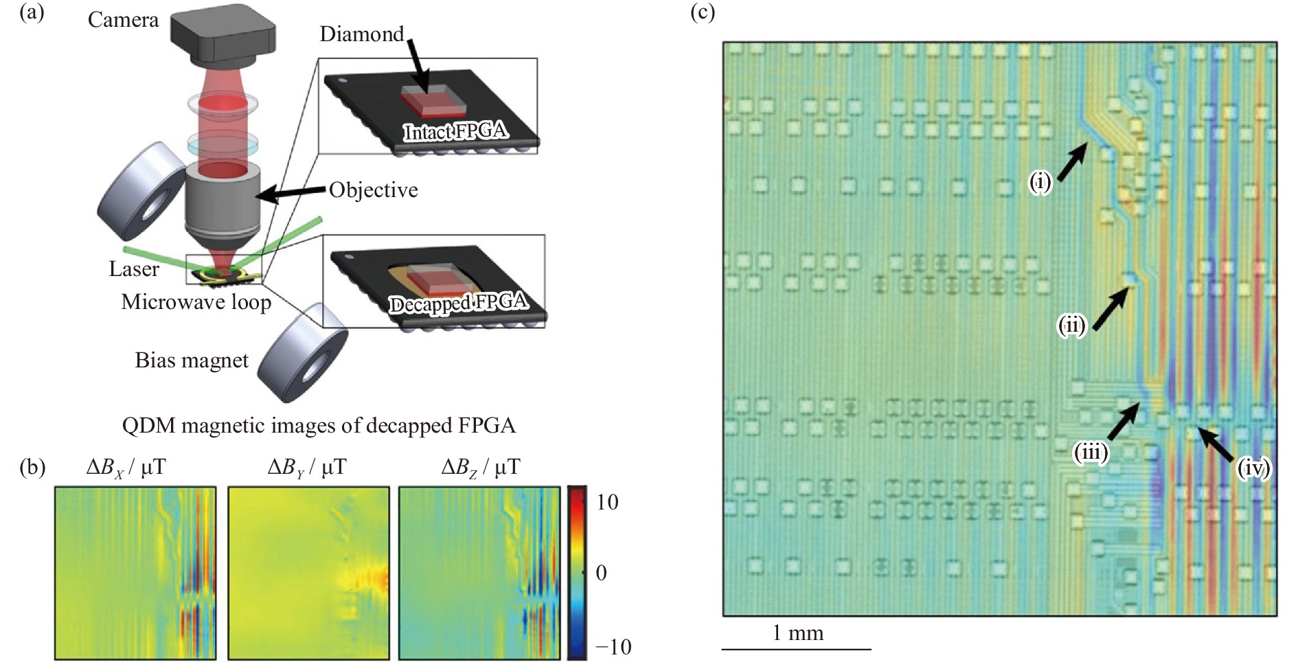
M.J. Turner, N. Langellier, R. Bainbridge, D. Walters, S. Meesala, T.M. Babinec, P. Kehayias, A. Yacoby, E. Hu, M. Lončar, R.L. Walsworth, and E.V. Levine, Magnetic field fingerprinting of integrated-circuit activity with a quantum diamond microscope, Phys. Rev. Appl., 14(2020), No. 1, art. No. 014097. doi: 10.1103/PhysRevApplied.14.014097
|
| [128] |
H. Rafii-Tabar, Computational modelling of thermo-mechanical and transport properties of carbon nanotubes, Phys. Rep., 390(2004), No. 4-5, p. 235. doi: 10.1016/j.physrep.2003.10.012
|
| [129] |
S.S. Zhang, Y.J. Wu, K. Luo, B. Liu, Y. Shu, Y. Zhang, L. Sun, Y.F. Gao, M.D. Ma, Z.H. Li, B.Z. Li, P. Ying, Z.S. Zhao, W.T. Hu, V. Benavides, O.P. Chernogorova, A.V. Soldatov, J.L. He, D.L. Yu, B. Xu, and Y.J. Tian, Narrow-gap, semiconducting, superhard amorphous carbon with high toughness, derived from C60 fullerene, Cell Rep. Phys. Sci., 2(2021), No. 9, art. No. 100575. doi: 10.1016/j.xcrp.2021.100575
|
| [130] |
P. Pachfule, D. Shinde, M. Majumder, and Q. Xu, Fabrication of carbon nanorods and graphene nanoribbons from a metal–organic framework, Nat. Chem., 8(2016), No. 7, p. 718. doi: 10.1038/nchem.2515
|
| [131] |
P.B. Bennett, Z. Pedramrazi, A. Madani, Y.C. Chen, D.G. de Oteyza, C. Chen, F.R. Fischer, M.F. Crommie, and J. Bokor, Bottom-up graphene nanoribbon field-effect transistors, Appl. Phys. Lett., 103(2013), No. 25, art. No. 253114. doi: 10.1063/1.4855116
|
| [132] |
E.Z. Shi, H.B. Li, L. Yang, J.F. Hou, Y.C. Li, L. Li, A.Y. Cao, and Y. Fang, Carbon nanotube network embroidered graphene films for monolithic all-carbon electronics, Adv. Mater., 27(2015), No. 4, p. 682. doi: 10.1002/adma.201403722
|
| [133] |
V.C. Tung, J.H. Huang, I. Tevis, F. Kim, J. Kim, C.W. Chu, S.I. Stupp, and J.X. Huang, Surfactant-free water-processable photoconductive all-carbon composite, J. Am. Chem. Soc., 133(2011), No. 13, p. 4940. doi: 10.1021/ja1103734
|
| [134] |
C.G. Zhang, J. Meng, K. Ma, X. Jiao, and Z.H. Yuan, A three-dimensional structure of ternary carbon for high performance supercapacitor, Diam. Relat. Mater., 109(2020), art. No. 108075. doi: 10.1016/j.diamond.2020.108075
|
| [135] |
C.H. Kang, C. Shen, M.S.M. Saheed, N.M. Mohamed, T.K. Ng, B.S. Ooi, and Z.A. Burhanudin, Carbon nanotube-graphene composite film as transparent conductive electrode for GaN-based light-emitting diodes, Appl. Phys. Lett., 109(2016), No. 8, art. No. 081902. doi: 10.1063/1.4961667
|
| [136] |
S.H. Lu, Y.C. Wang, H.Y. Liu, M.S. Miao, and Y.M. Ma, Self-assembled ultrathin nanotubes on diamond (100) surface, Nat. Commun., 5(2014), art. No. 3666. doi: 10.1038/ncomms4666
|
| [137] |
P.B. Li, Z.L. Xiang, P. Rabl, and F. Nori, Hybrid quantum device with nitrogen-vacancy centers in diamond coupled to carbon nanotubes, Phys. Rev. Lett., 117(2016), No. 1, p. 015502. doi: 10.1103/PhysRevLett.117.015502
|
| [138] |
K. Kaiser, L.M. Scriven, F. Schulz, P. Gawel, L. Gross, and H.L. Anderson, An sp-hybridized molecular carbon allotrope, cyclo[18]carbon, Science, 365(2019), No. 6459, p. 1299. doi: 10.1126/science.aay1914
|
| [139] |
J.T. Wang, X. Jin, Z.B. Liu, G. Yu, Q.Q. Ji, H.M. Wei, J. Zhang, K. Zhang, D.Q. Li, Z. Yuan, J.C. Li, P. Liu, Y. Wu, Y. Wei, J.P. Wang, Q.Q. Li, L.N. Zhang, J. Kong, S.S. Fan, and K.L. Jiang, Growing highly pure semiconducting carbon nanotubes by electrotwisting the helicity, Nat. Catal., 1(2018), No. 5, p. 326. doi: 10.1038/s41929-018-0057-x
|
| [140] |
T. Lei, L.L. Shao, Y.Q. Zheng, G. Pitner, G.H. Fang, C.X. Zhu, S.C. Li, R. Beausoleil, H.S.P. Wong, T.C. Huang, K.T. Cheng, and Z.N. Bao, Low-voltage high-performance flexible digital and analog circuits based on ultrahigh-purity semiconducting carbon nanotubes, Nat. Commun., 10(2019), art. No. 2161. doi: 10.1038/s41467-019-10145-9
|
| [141] |
K.S. Novoselov, V.I. Fal′ko, L. Colombo, P.R. Gellert, M.G. Schwab, and K. Kim, A roadmap for graphene, Nature, 490(2012), No. 7419, p. 192. doi: 10.1038/nature11458
|
| [142] |
J.W. Liu, H. Ohsato, M.Y. Liao, M. Imura, E. Watanabe, and Y. Koide, Logic circuits with hydrogenated diamond field-effect transistors, IEEE Electron Device Lett., 38(2017), No. 7, p. 922. doi: 10.1109/LED.2017.2702744
|
Figures(8) / Tables(2)

Copyright © 2019 Editorial Office of International Journal of Minerals, Metallurgy and Materials 京ICP备13030111号
Supported by:
Beijing Renhe Information Technology Co. Ltd
Email:
info@rhhz.net


 Search


 DownLoad: